Microarchitectural Blueprint & Memory Hierarchy
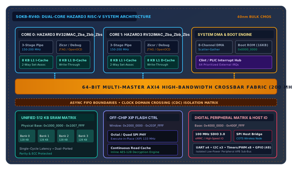
Detailed breakdown of SOKB Semiconductor's dual-core RISC-V SoC subsystem, 64-bit non-blocking AXI4 crossbar, unified zero-wait SRAM subsystem, and asynchronous clock boundary isolation.
Full SoC Interconnect & Macro Layout
SCHEMATIC BLOCK DIAGRAM: SOKB-RV40-RTL
System Memory Map Architecture
Deterministic, flat 32-bit physical memory map designed for bare-metal execution and deterministic RTOS schedulers (FreeRTOS, Zephyr). Click any address block to inspect bus protocol and cache coherency rules.
| Physical Address Range | Memory Region | Size | Bus Target |
|---|---|---|---|
| 0x0000_0000 - 0x0000_3FFF | On-Chip Boot ROM | 16 KB | AHB-Lite / AXI |
| 0x1000_0000 - 0x1007_FFFF | Unified System SRAM Matrix | 512 KB | 64-bit AXI4 Crossbar |
| 0x2000_0000 - 0x203F_FFFF | Off-Chip OSPI/QSPI Flash XIP | 4 MB Window | Octal SPI PHY |
| 0x4000_0000 - 0x400F_FFFF | Digital Peripheral Register Space | 1 MB Space | Async APB4 Bridge |
All bus accesses below 0x1000_0000 require privileged Machine (M) mode privilege levels during boot phases. Non-privileged code execution triggers precise Machine Trap interrupts to the PLIC.
The Phase 1 FPGA Digital Twin Sandbox
To eliminate financial exposure before committing millions of rupees to 40nm photomasks, SOKB Semiconductor deploys an exhaustive FPGA Digital Twin Framework. The entire processor matrix, AXI4 crossbar, cache controllers, and peripheral macros are authored exclusively in technology-independent generic SystemVerilog and Verilog-2005 RTL.
By avoiding vendor-locked primitive macros (such as proprietary Xilinx DSP blocks or vendor-specific BRAM instantiations), the exact same synthesizeable codebase compiles seamlessly into Xilinx Kintex-7 / AMD Zynq UltraScale+ FPGA emulation boards as it does into Synopsys Design Compiler targeting foundry standard cell libraries.
- RISCOF Architectural Compliance: Full RV32IMAC conformance verified across > 12,000 formal instruction sweeps.
- Verilator 2-State Simulation: Rapid C++ model generation achieving > 1.5 MHz cycle speeds for bootloader development.
- Cocotb Python Testbenches: Asynchronous burst stress tests on the AXI4 multi-master matrix verifying zero-deadlock guarantees.
- Physical Hardware Loop: SPI/SDIO wired to physical COTS Wi-Fi/Bluetooth transceivers running live IP stacks.
Timing & Synthesis Vectors: Asynchronous FIFO Isolation
Dual-Clock Domain Crossing (CDC)
The high-speed compute engine operates at 150-200 MHz, while serial peripheral lines (UART, I2C, SPI) operate on fractional 10-50 MHz clocks. SOKB employs dual-clock Gray-coded asynchronous FIFOs with 2-flip-flop synchronizers to guarantee a Mean Time Between Failures (MTBF) exceeding 100,000 years against metastability.
Static Timing Analysis (STA) Corners
Sign-off timing is validated using Synopsys PrimeTime across extreme PVT corners: Slow-Slow (0.99V, 125°C junction temperature) for setup timing closure and Fast-Fast (1.21V, -40°C) for hold time margin validation. Zero setup/hold violations are enforced across all multi-cycle paths.
Synopsys Design Compiler Synthesis
Mapped to standard 40nm 9-track high-density standard cell libraries with automated clock tree synthesis (CTS) inserting balanced inverter buffers. Dynamic power is minimized via automatic fine-grained clock gating on unselected register files and idle cache lines.